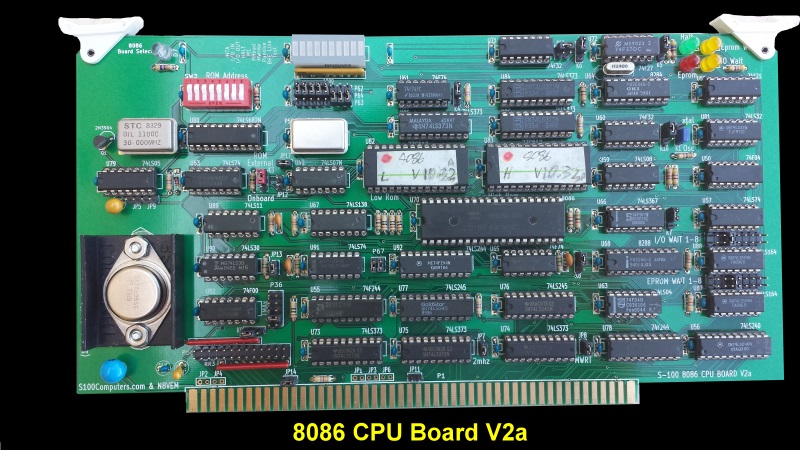
S100 Computers

Home S-100 Boards History New Boards Software Boards For Sale
Forum Other Web Sites News Index    
  
An S-100 8086 CPU Board.
  
  Final 8086 CPU Board

INTRODUCTION
A number of the later S-100 board manufactures had their own 8086 CPU card.  Some had dual Z80/8088 CPU boards. There were even a few 8 bit 8088 S-100 CPU boards.  These boards moved the S-100 bus capabilities into the 16 bit world. Software was usually either CPM86 or a variation of MS-DOS.  This was at the time the IBM-PC and PC clones began to dominate the area and so IBM-PC compatibility became the rage. Few succeeded in true software/hardware compatibility. Only CompuPro or Lomas based board systems came close to achieving this goal.  One of my goals will be to do this.

I built a very early S-100 8086 prototype board back in the early 80's.  Here is a picture of that board:-

8086 Prototype Board
The board was configured in the 8086 "MAX" configuration so it could accommodate an Intel 8089 I/O coprocessor and Intel 8087 math coprocessor. The board (still) works well up to about 5Mhz in my system.  It runs fairly hot however with these old chips -- thus the heat sinks attached to each chip!  Because of space limitations there was no on board monitor EPROM. Instead the board booted directly from RAM/ROM on the S-100 bus at FFFFF0H.  BTW, this is where our Z80 CPU board with its ability to address 1MG of RAM came in real handy. Because one can easily deposit 8086 code at that area in RAM for board testing etc.  Considering the fact that this was a 3 chip set, it has remarkably few IC to work in an S-100 system. This is to some extent due to the fact that the S-100 bus is really geared to an Intel type of hardware system.  The board turned out to be very reliable and allowed me to develop much 8086 software. I installed both CPM86, the unofficial upgrade CPM86+ and MSDOS using this board. 

However I felt any new S-100 8086 board should be capable of running at a higher speed, something in the range of 8MHz using the later 8MHz chips.  Consequently I modified the above board fairly extensively.   I decided not to include the two coprocessors. I reasoned that anybody needing this capability will be using an 80286 or 80386 S-100 board (future boards, later this year).  Instead I decided to place an onboard pair of EPROMS on the board.  Using the schematic shown here, I drew up the following early prototype. Here is a picture of that board:-
  
  V2 Prototype Board
     
Here is a schematic for this board.  There are more support chips on this board because we are now including the two EEPROMS. As we shall see below these two chips require their own address and data buffers (5 chips).

BTW, if you wish to understand the 8086 CPU in detail an outstanding source of information is the Osborne/McGraw-Hill 1980 book: "The 8086 Book" by Russell Rector & George Alexy. The Intel Data sheet can be seen here.

Let us look at the boards components one at a time. 
 
The Master/Slave Transfer Logic
This board upon power on or reset will normally exist on the S-100 bus as a slave CPU board. That is it will be inactive while the Master CPU (usually a Z80) board is active. (It can be configured as a Master itself, but lets pass on this for now).   Please look at this diagram.
   

Reset Circuit
   
As setup the Intel 8284 "Clock Controller" holds the 8086 in a permanent reset state (pin 11 is low).  The S-100 bus allows for up to 16 slaves (CPU/DMA) boards. They are selected by the four S-100 lines TMA0-3 (pins 55-57 & 14).  I will use the TMS0 line here.  To activate the board we lower TMA0 (typically by outputting a bit from a port elsewhere on the bus, e.g. the SMB, but this could even be a bounce less switch).  This lowered signal is passed along step by step the three 74LS74 flip flops A,B & C. A and C are clocked by the S-100 bus master clock Phi.  The output from flip flop A is sent back to the bus as a low on the S-100 line HOLD* (pin 74). This tells the Z80 another board wants the bus. When it is ready it raises the S-100 hold line pHLDA which clocks the flip flop B. This is then clocked (by Phi) through flip flop C and eventually raises the Res* pin 11 on the 8284. This releases the 8086 from its reset state. The output of flip flop B also puts out the important signal XFERII which amongst other things allows the "new" Phi clock signal for the 8086 to appear on the bus.  Meanwhile at this time all the Z80 status, data, address and control lines are tri-stated.  It's as if the Z80 no longer exists on the bus.

Now it should be pointed out that the original IEEE-696 specs allow for only 1 master clock on the bus. In real world practical systems this usually meant the Z80 clock.  It was not long however until almost every S-100 board manufacture  adapted a modification (like that above) that allowed the slave CPU to supply its own (faster) clock.  This is what I will use in all our Slave S-100 boards.  It is important also to remember that this board cannot itself transfer control to another slave board (for example a DMA controller) the board/software must refer back to the true S-100 bus master.  This is how the IEEE-696 protocol was setup.

Intel allowed two sources for the actual clock frequency generation. A crystal connecting to pins 17 & 17 of the 8284 or a clock oscillator connected to pin 14. Pin 13 determined the source.  In both cases the input frequency is 3X the desired output frequency.   For flexibility, I allow both sources to be used. I started with a 24Mhz crystal.

Status and Control Lines
It is absolutely critical that the above transition takes place in an orderly fashion where at no time are any of the S-100 bus lines left floating -- no matter how short the time.  This is accomplished in a two step process called XFERI and XFERII.  In XFERI the Z80 bus status, data and address lines are switched over to the 8086 but the Z80 still retains control of the critical control lines pSYNC, pWR*, pDBIN and pSTVAL*.   In this way even though all the other S-100 lines are getting switched over nothing will happen to any of the S-100 boards (if they are IEEE-696 compatible).   No memory will be written to with garbage, no ports accessed etc.  When that transfer is complete, only then, does the second XFERII process take place.  For a very brief period of time the Z80 and 8086 will BOTH be controlling the pSYNC, pWR*, pDBIN and pSTVAL* lines.  (That is why on well designed boards they have 10 Ohms resistors -- to protect the bus drivers).   Once the Z80 signs off (one Phi clock cycle later), the 8086 has complete control of the S-100 bus.
    
Control Lines
  

This whole process seems complicate at first and to some extent is,  but a lot of thought, care and attention was put into it by the original IEEE-696 committee to allow for an extremely reliable system.

If you don't quite understand the above, don't worry just look upon the circuits as a "black box" for Master/Slave switching. 

The actual generation of the critical 8086 control signals is relatively straightforward. Intel did a good job of presenting a simple symmetrical set of signals. First look at the following diagram:-

Control Generation

First it should be stated that  the 8086 actually can be configured in two different configurations. A "MIN" and a "MAX" mode depending on the status of pin 33. If pin 33 is high the 8086 configures itself in the MIN mode. This configuration is meant for simple 8086 applications where there is a minimal (if any) bus structure and no co-processor support.  The memory and port control lines come directly from the CPU.  The MAX mode is different (pin 33 to ground),  in this case the 8086 configures itself for a multi-processor arrangement with a bus structure and possibly co-processors.   The control lines do NOT come directly from the CPU but instead three lines S0, S1 and S2 send encoded information to a special "Bus Controller" called an 8288, (see here for specs).  This chip interprets the S0-S2 signals and puts out the appropriate Memory/Port RD/WR signals.  The interpretation is fairly straightforward and can be summarized as follows:-

S0-S2 Table

As you can see we have all the raw information we need to generate the S-100 bus signals.  All we have to do is construct a pSync and pSTVAL signal.  In fact a simple 74LS138 will get you a similar set of signals. We could in fact do away with the 8288 entirely except for the fact that that chip  does put out a special "Advanced" memory write control and "Advanced" I/O control that allows the system get an earlier signal than would be available with S0-S2 alone. This give us more memory and I/O access times.  This alone would probably not be a reason enough for adding this extra chip. I use it because as we shall see when we later move up to a 80286 board we will absolutely need a bus controller chip. May as well get the bugs worked out on a simpler system!  Nevertheless I do use a 74LS138 (U67) to control an LED bar at the top of the board.  The LED's in the bar (left to right) individually signal when the 8086 state is:- INTA, I/O-IN,  I/O-OUT, HALT, an M1 Cycle, MEM-READ,  MEN-WRITE, and PASSIVE.  These are quite useful when you single step the CPU in the S-100 Bus.

The outputs of the 8288 are combined to yield the appropriate S-100 signals and placed on the bus via U56.

Data and Address  Lines
The 8086 multiplexes its 20 address lines and 16 data lines. Both come from the same set of pins on the CPU.   This complicates things slightly. For each bus cycle the address lines are first presented. They must be latched into the Intel 8282's (U73,U74 & U75) with the ALE (Address Latch Enable) from pin 5 of the Bus Controller (the 8288).  Only later does the DEN (Data Enable, pin 16) signal appear which activates the S-100 data bus drivers, Intel 8286's (U76 & U77).  The Bus Controller signal DT/R (pin 4) determines the direction in which the data flow is expected (to the CPU or to the S-100 Bus).
Here is a summary of the layout:-

Address Lines

This two step multiplexing of address and data slows the 8086 down and was done away with in the later 80286 chip.  Nevertheless when done properly it is very reliable.

All this would be fairly straightforward if it was not for the fact that the 8086 will input and output either 8 or 16 bits of data.  The special sXTRQ* of the S-100 bus must be handled to let other boards on the bus know what to expect.   I have discussed at length elsewhere on this site this process. See here.  Fortunately the 8086 has a special pin BHE (Bus High Enable) which greatly simplifies this process. Pin 16 of U84 delivers sXTRQ*  to the S-100 bus.  

The 74LS244, U78, takes care of the transferring both memory and port ODD address IN  8 bit data (or interrupt return vectors - typically from an 8259, see here) to the lower byte data bits of the 8086 where it expects to find them.  The circuitry took quite some time to figure out and for most is best looked upon as a "black box".


The Onboard EEPROM  
As I said above, my original prototype board did not have an onboard ROM.  Instead after a reset it looked at the S-100 bus RAM at FFFF0H.  There are some advantages to this. With a Z80 system that can examine and modify RAM at this location (see here) you can quickly test a board. This will be described below in detail.  However there are advantages to having a powerful on-board EPROM monitor on the board -- particularly if it is to be a bus master and the only CPU in a system.

Unfortunately adding an EPROM takes more space than you might expect.  In order to simplify the hardware, first we use two EEPROMS, a high and low byte.  This avoids the need for a BHE pin function since the 8086 will never be a write to this memory location,  (the CPU itself takes care of the data lines for High/low input data). However we do need to latch the address lines as we do for the "normal" S-100 address lines. Furthermore whenever the 8086 is addressing the onboard EEPROM it must inactivate completely the drivers to the actual S-100 bus.   The EPROM_SEL* signal generated as shown in this schematic does this:
  
EEPROM Circuit
   
Note how the outputs from the data pins of the two EEPROMS directly drive the data pins of the 8086 once ROMRD* is low.  Note also how EPROM_SEL* inactivates the S-100 drivers in the above previous schematic.  With SW3 the EEPROM can be configured to many different sizes, we will typically take up only the top 64K of the 8086's 1M address space.


A FINAL PROTOTYPE 8086 BOARD
Much was learned from the above board.  It worked very reliably at 6MHz but was unreliable above that.  I went through two further prototype boards to arrive at this final prototype board which I am quite happy with.

V3 Prototype
Most of the changes are minor and subtle. I will not spend much time recalling some frustrating experiences tracking down bugs.  The schematic of the final board can be see here.  Amongst the changes were:-

  Switched bus drivers from Intel 8282's & 8286's to the more common (and far less expensive), 74LS373's and 74LS245's.
  Completely redid the wait state circuitry (allowing 0 to 8 weight states) for slow old  I/O boards and the onboard EEPROM/ROMs
  Adding on the board an IO port board circuitry that allows any CPU to switch on the board (no longer need the SMB or an external switch).
  The board can now utilize either 27C512 (or more practically) 28C64 EEPROMS
  More LED's to show what is going on.

The board in my hands will work (at 8MHz - see below) with any of the S100Computers board we made over the years. It also works with a number of IEEE-696 Memory boards such as the CompuPro 128K static RAM-21 board, the 256K static RAM boards from BG Computers or Fulcrum and the Electrologics 1MG Memory Disk.  I have not tested it with any Dynamic RAM boards. If these boards have their own onboard refresh controller I suspect they would be fine -- at least up to 6MHz.   If however they rely on the Z80 refresh signal (non-IEEE 696 boards), they defiantly will not work.

For the board to run at 8MHz it has to be jumpered for (at least) two wait states for I/O in order to utilize I/O ports on other S-100 boards. Also for reliability a number of the 74LSxx chips need to be changed to the faster 74Fxx types.  These are indicated in the schematic. The Achilles heel of the board is for fast 8 bit reads of memory from odd address lines. The S-100 bus brings this 8 bits of data in to the board on the upper 8 bit (S-100) data lines.  They must be shifted down to the lower 8 bit data bus via U78 and then passed through U75.  This unfortunate "in, across, and then in"  process has a slight timing overhead, so it is important that the logic involved is fast. Thus the use of 74Fxx chips in these areas (U52, U60, U72, U58, U71, U78) on the board.

Realizing that people may wish to use this board with old S-100 boards that have slow I/O access times (old IMASI/Altair 2MHz systems) I added the following circuit that allows up to 8 wait states to be inserted during any S-100 bus Port I/O.

Wait State Circuit

The IOWAIT line feeds into the RDY line of the 8284 clock generator.

Here are some logic signals on from the board with 0,1 and 8 Wait states:-

Wait States

BTW, don't worry about the irregular top clock pulses. The reason they vary a little is because the data access rate of the PC based logic analyzer cannot keep up fast enough. The data analyzer gave the WR* pulse width at 8MHz with 0-4 wait states as:-

0 = 125 ns, 1 = 208 ns,  2 = 291 ns, 3 = 375 ns, 4 = 416 ns

Please note because of the way the wait circuit is set up the jumper p65 1-2 and p66 10-2 act as if there is no jumper. One wait state starts at p65 2-3 or p66  2-3. With this board you can go up to 7 wait states! More than 4 however is probably not practical.

The board can be "single stepped" on the S-100 bus using for example our SMB board.  It is important to remember however that the 8086 has an internal 6 byte "look ahead" queue, so the status signals on the bus actually are slightly ahead of what the 8086 internally is doing. Normally this is not seen -- unless the queue is jumped by an opcode like JMP.  The 10 panel LED Bar at the top of the board indicate the current 8086 cycle.  Here is the breakdown:-

LED Bar
If you put the following code in RAM at FFFF0H:-

B0, 33, E6, 01, EB, FA

and jump to it (reset point for 8086), The 8086 will continuously out the ASCII latter '3" on the console port 1. If you have the S100 Computers SMB and single step the 8086 you will see the appropriate LED's come on as indicated above.

The fourth from the left LED bar is useful as we shall see in building the board. If you fill a ROM with 8086 "HALT" instructions (F4H). It should be the only bar lighting up if the 8086 reads RAM/ROM correctly. This test is independent of any even/odd 8 or 16 bit logic on the board.

The board will work with older 8086's (and 8284's & 8288's) at 6MHz.  To reach 8MHz you need the equivalent chips. The 8MHz Intel chip is called 8086-2.  However these Intel chips do run hot. It does not seem to bother them, but I always like to run cool boards in my system. Consequently I normally use the CMOS equivalent chips. I use the NEC V30 chip. This is a completely hardware equivalent CMOS chip to the Intel 8086 and is in fact rated for up to 16MHz!.  I use the CMOS equivalent 82C84 and 82C88 support chips as well.  These run almost cold. The boards Voltage regulator is only warm.  A good source of these chips is Unicorn Electronics.  The V30 is harder to find, though they are usually on eBay. I got mine from a friend.


Final 9 MHz Master 8086 CPU Board.
The final (V3) of this board is now completed and people have received boards.   Some minor tweaks of the above V2 prototype board were made. In particular we reassigned some gates and removed  empty sockets. This allowed considerable trace optimization. The final schematic and board layout are shown at the bottom of this page. 

The board in my bus actually "works most of the time"  at 10.5 MHz. However it's not completely reliable at these speeds.  Some day I may try tweaking the above chips some more.  At 9 MHz it's completely reliable using 2 I/O wait states (and 3 EEPROM wait states) with the S-100 boards I have described on this web site. This is using the NEC V30 CPU instead of the Intel 8086-2 chip set.  The Intel chip is good for 8MHz but as I described above, runs hot. Try and use the CMOS chips if you can.

Here is a picture of the Final 8086 Master CPU Board.
Final CPU Board
  
As we will see below the board runs rock solid with the S-100Computers ZFDC Floppy disk controller, and the IDE Board for CPM86 and MSDOS v4.01 at the above speeds.


Step By Step Building The Board.
Since for many this board may be their first venture into putting a 16 bit system in their S-100 bus I will go into some detail as to how to get it up and running and while next year we will be moving up to 80286, 80386 and 68K CPU boards it is really important to have a basic S-100 16 bit CPU board you can fall back on to debug these more complicated systems.

The first step is to examine the board carefully for scratches or damaged traces. Use a magnifying glass if need be. The quality of the boards we get is excellent. I must have done 30 by now, never had a problem, but there is always a first time. A broken trace is almost impossible to detect by eye on a completed board.

Next solder in all the required IC sockets, resistors, resistor arrays, capacitors, jumpers, the 24MH crystal, SW3 and the voltage regulator.  Do not add the LED's or LED bar yet. Be sure you put the resistor arrays in with the correct orientation of pin 1. Check their values before  soldering (they are difficult to remove).  You may want to consider/check using a 470 Ohm array for RR4 instead of 1K depending on how bright you wish the LED bar to be.

For prototype boards I generally use "double swipe" IC sockets. For a critical board like this I prefer to use "Machine Tooled" IC sockets.  However they are more expensive and you have to be particularly careful not to bend the IC pins.  If you think you will be doing a lot of EEPROM burning you should use the Low Profile ZIF sockets (e.g. Jameco #102745) for the two EEPROM sockets.  The two clock oscillators should have their own special sockets (e.g. Jameco #133006).

Check the voltage to sockets on the board is above 5V by placing the board in your S-100 system using an extender board. With no load you will typically get 5.25V.  BTW, your system should boot and run correctly with its Z80 CPU. If not, you have a serious solder bridge somewhere on the board.  Before you do anything else with a magnifying glass go over every socket on the board and examine for a proper solder joint. I like to "reheat" each joint just to be on the safe side. The silk screen/varnish on these boards us quite thick. It's easy not to have a good solder joint for the ground pins.  Double check.   Extra time here will save you hours later!

We will now build the board up in functional steps. Avoid the temptation of adding everything at once and popping it into your S-100 box. Step by step is faster in the end -- trust me.

First we will add the 5 LED's.  Insert LED D7 into the board (usually the longer lead into the square pad) but do not solder yet.  Insert the board into your S-100 system and with a probe tied to +5V touch pin 3 of IC socket U66. The LED should light up. If not switch the LED leads.  Only then solder in place.  Repeat for LED's D2, D6, D5, and D3 only this time ground the appropriate pins of U66. Solder the LED's in place and recheck.

The color of the LED's is up to you. I always use blue for "board select" in my system so LED D7 is blue.  Since D2 and D6 are for wait state indications I use the same colors (yellow).  D6 is on when the EEPROM is being used so red and D3 is only active if the 8086 is in HALT mode so it is green.

Next we will add the circuit that switches the board from a dormant state on the S-100 bus to an active slave.

Jumper P67 1-2 and 3-4 (Vert.)   and P36 1-2 (Horz). While on jumpers, please note every time when we talk about jumpers,  position 1 is the square pad of the jumper. In order to minimize board trace lengths, its actual position/orientation on the board will differ from jumper to jumper.  Sometimes they are top to bottom or left to right, other times the exact opposite.  An incorrect jumper can be a real pain in debugging a non-working board. Check with the schematic each time, to be sure . Make sure you correctly identify pin 2 in each case.

Next add IC's U52, U89, U90, U91, U49, U71,  U92, U55, and U56.

Insert the board into your S-100 system and with your Z80 monitor input port EDH.  (This will be our default port to switch out the Z80 and activate the 8086 board on the bus).  The jumper on P36 should switch from high to low.  Input again, it should go back high.  Note just in case you have port EDH assigned to something else in your system, jumper P67 also allows you to also use DDH. 
   
At this point you can now add the 2 MHz Oscillator  and U79.

Next we will add the complicated but critical handshake circuitry that switches this board on to the S-100 bus as the current bus master.

Check we have the above jumper P36 1-2.  Add  P57 2-4 (Horz),  JP17, JP12, K9 2-3, JP7, K10 2-3 and JP8
Next add U50, U53, U57, U59, U66, U60

Input port EDH again the LED D7 should light up. However this time the Z80 will be in a hold state and will not respond to any commands. If you are using my Master Z80 Monitor use the "W" command.

Here is a picture of the board at this test stage:-
 
Port Test
  
Next add the 27 MHz Oscillator and 82C84 (U64) clock controller. Set K1 1-2 (for oscillator not crystal source). Note the 8284 clock controller takes a 3X Oscillator or Crystal. So 9X3 = 27 MHz.  Of course you can use a slower Oscillator if you like. I just happen to have more Oscillators than crystals!

Add U58.  With a logic probe check for a clock signal on pin 19 of socket U70 and pin 22 of socket U70 is high.   Activate the board and check pin 21 of socket U70 goes from high to low and pin 22 stays high.

Next we will add the wait state generators. Please note there is a silk screen error on the board where the "EPROM WAIT 1-8" and I/O Wait 1-8" were switched. (Its cosmetic, P65 sets EPROM wait states, P66 sets I/O wait states)
Add U87, U88 and U81.  Jumper p65 (labeled I/O Wait 1-8) 5-6. Jumper p66 (labeled EPROM Wait 1-8) 7-8.
Repeat the above test. The LED D7 should still light up.

Next add U63 and jumpers JP 13 & 14. Set jumper K4 2-3.  Activate the board and check pins 18,17 and 23 of socket U70 are all low.
Insert the LED bar do not solder and check the right most bar lights up. If not check the LED bar orientation and solder in place.

Next we will insert the critical CPU control and status lines circuitry.
Insert U67, U68 (the 82C88) , U61, U72 and U65.
Jumper K8 1-2.
Activate the board. The "Passive bar" should light up. See the picture above that describes the LED bar.

Next we will add the onboard EEPROM circuitry.  We will setup the board for two 28C256 EEPROMS (but only use part of the total ROM space for our monitor code residing at FC000H-FFFFFH, see below). 
Add U80.
Jumper P62-P64 1,2,3,4,5 and P64-P63 6,7,8.
Jumper K3 1-2, K5 2-3, K6 2-3 and K7 2-3.
Set SW3 1-5 open, 6-8 closed.
Activate the board, LED D5 should light up. 

Here is a picture of the board at this stage:-
 
Passive Mode test
  
Next we will add the drivers for the onboard EEPROM
Add U85, U86, and U84. Repeat the above board activation test (input port EDH).

Next we will add the 8086 drivers.
Check pin 1 of socket U78 and pin 19 of sockets U77 and U76 are all high before adding these IC's.   If not find out why before going further. 

Next check pin 1 of sockets U55 and U56 are high. If so add U55 & U56. Do NOT activate the board in the S-100 bus.
Next add all remaining IC's to the board (U73, U74, U75 and the 8086 CPU U70). 
Jumper K1 2-3, Do NOT activate the board in the S-100 bus.

We are now ready for the big event -- let the 8086 CPU control the bus.  Remember the 8086 boots up from a reset at FFFF0H in RAM. What we have there determines what the CPU will do after a reset.

There are a number of ways you can go from here.  If you have one of our S100Computers  Z80 CPU boards (or the Intersystem's Z80 Series-II board) and 16 bit RAM at the top of the 1MG address space (e.g. our 4MG static RAM Board) you can program the RAM with the code described below, forcing  this board not to  boot from the onboard EEPROMS (Jumper K3 2-3).

Alternatively you can burn the code described below into two EEPROMS.  Remember however that these EEPROMS must separately contain the low/even bytes and high/odd bytes of code.  Fortunately most EPROM programmers have this option. I really like the Weldon VP-280 type programmers. They are Windows 7 compatible and very easy to use. See here.   The low byte socket is on the left hand side of the board.

OK let's take the plunge. There are 3 simple pieces of 8086 code that are your best friend! 

HALT's.

Whenever the 8086 sees a halt instruction (a single byte F4H) in RAM/ROM it will stop everything and remain there until reset.   So the first thing we will do when we put together the board is have it see memory with just F4H's.  It must halt. The above 3rd from left LED bar must come on (as well as the special HALT LED D3).  This process is independent of any Odd/Even address or in fact any RAM/ROM location.   You must get this working before going further.  So fill RAM or burn EEPROMs with F4's as your first test. The board after getting control of the bus MUST display the HALT LED bar. Do not go further until you get this to work.


Next we will write a very simple routine to continuously output a character on the CRT.

(B0, 33, E6, 01, EB, FA)
START:  MOV    AL,33H
              OUT    01H,AL
              JMP     START


You will typically place this code at FFFF0H in RAM or ROM.  This the start reset address of the 8086 at the very top of its 1MG address space. This code is position independent but does require a functional Odd/Even address circuit to work. If all is well you will see continuous letter "3" on your console (assuming it is at port 1H). 

As I said above you can burn two EEPROMS with the above code or with our Z80 board switch in the top 4K or the 1MG address space to 0H in RAM and add the code at 3FFF0H. Use:-

QO D2, FC                               ;Temporally allow the Z80 to access RAM at FC000-FFFFFH at 0-3FFFH
S3FF0  B0,33,E6,01EB,FA         ;Insert the above code at FFFF0 in RAM
QI ED                                      ;Inputting port ED activates the 8086.

The advantage of this approach is you don't have to burn any 16 bit pairs of ROM's.  The memory board (if its IEEE-696 compatible), will take care of the odd/even byte addressing for you.        

Next we will place the above code in RAM at 500H and in our EEPROM program the 8086 to do a FAR Jump to 500H upon reset.  We do this by putting the following code at FFFF0H:-


(EA 00 05 00 00)
         JMPF      500H

This will test your boards ability to read RAM reliably.  This BTW is where we will place the CPM86+ boot code.  If you get this latter piece of code working you are well on your way of having a hardware functional S-100 8086 board.

If you see the letter "3" being continuously displayed on your CRT you are almost done. The board is working fine.  You may have to play around with wait states or drop the clock speed.  With Jumper K1 set 2-3 the 82C84 is using the 24MH crystal as a clock source. If you jumper K1 1-2 you can try various oscillators as a clock source. Start at a slow speed say 6MHz.

Bringing up a 8086 Monitor,  CPM86+ and MSDOS with this 8086 S-100 Board.
To be of any use we clearly need a disk operating system to work with this board.  There are really two options: CPM86 or some type of MS-DOS. I have used both in the past.  However again realizing this may be a dramatic step for people coming from the 8 bit world, I will start with a 8086 Monitor for the onboard EEPROMS and then "do" CPM86+.  Please click here to get to the 8086 Monitor software section of this web site for the 8086 Monitor details,  or the CPM86+ section for step by step instructions about bringing up CPM86+ on a CPM(80) system for the first time. 

Remember if you are using a 28C256 type EEPROM you need to place the 16K 8086 monitor in the top half of the 32KX8 EEPROM.  Please review the write-up here if you need more help on this topic.

Much work has gone into writing the 10,000 line 8086 monitor code so it is compatible with MSDOS.   As it currently stands the 8086 monitor below will allow you to boot MSDOS v4.01 from our ZFDC controller board and/or IDE CF card board unaltered as they are supplied by Microsoft using this board.   A description of this is given elsewhere here and really requires you study the monitor code itself in some detail.

Link to 8086 Monitor and Video Describing the Board & booting MSDOS with it.
Link to CPM86+

A Description of the Board Jumpers.
The  board contains a number of important jumpers that determine how it functions. Most will not need to be changed once the system is running but it is very important they are configured correctly.  In no particular order:-
   
Jumper    Function 
JP5,JP6,JP4,JP9 Used only if the board is to act as a bus master.  Generates Power On reset etc.
JP12 Use only if no other board on the bus pulls up the S-100 HOLD signal
JP11 Use only if no other board on the bus pulls up the S-100 HLDA signal
K9, K10 Normally 2-3. Use 1-2 if board is a bus master.
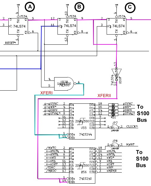
JP7 Use only if no other board generates the S-100 2MHz clock signal when the 8086 is active
JP8 Use only if no other board generates the S-100 MWRT signal when the 8086 is active
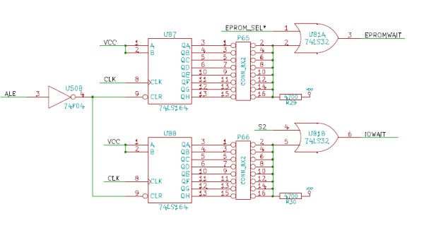
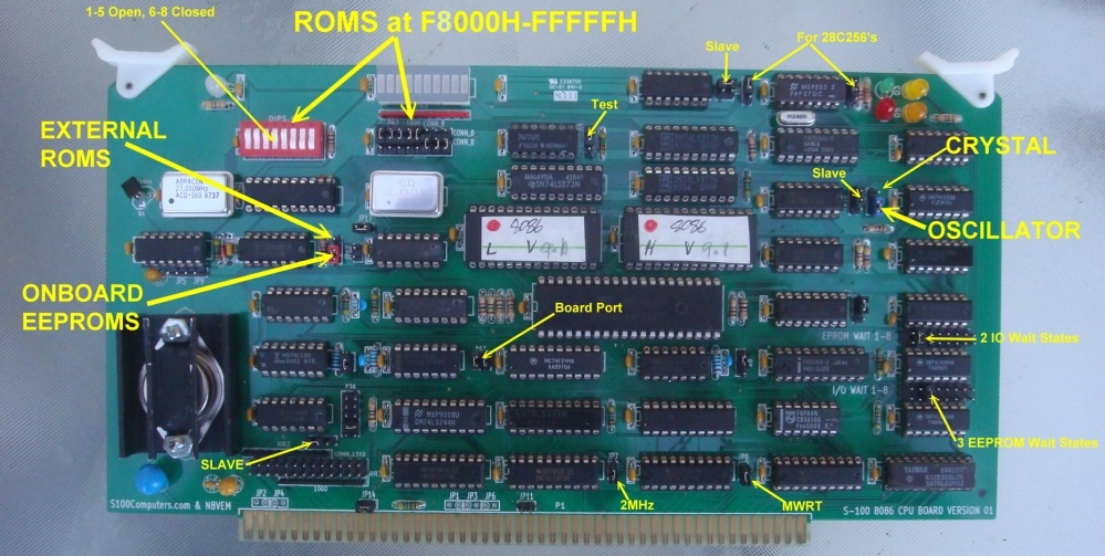
P65 Sets number of wait states for onboard EEPROM (0-8). I use 3 wait states, so P65 5-6
P66 Sets number of wait states for bus I/O and INTA cycles (0-8). I use 2 wait states, so P66 3-4
P57 Normally set 2-4. Use 1-3 if board is bus master
K8 Normally 1-2. If set 2-3 control signals appear on bus a little before pSync ends.
P36 Determines what S100 TMA line activates this board.  (Normally TMA0* from SMB, so P26 3-4. For onboard activation use 1-2 & 3-4) 
P13, P14 Use only if no other board on the bus pulls up these signals
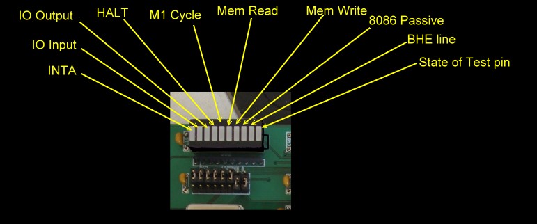
K4 Normally 2-3. This controls the 8086 special test/debugging pin
K1 1-2, Oscillator supplies CPU clock. 2-3 Onboard crystal supplies clock
K3 Normally 1-2. If set 2-3 the onboard EEPROM circuit is invisible to the 8086.
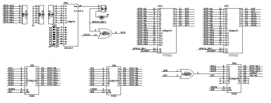
K5, K6, K7 These pins must be carefully selected for different EEPROM and EPROM types (see below)
P67 Normally 1-2 and 3-4. This selects the port to activate the 8086 board on the bus.
P62-P64 & SW3 This selects where the onboard EEPROMS will reside in the CPU's 1MG address space
P56 1-26 These jumpers are to pull up the S-100 bus Interrupt and DMA lines IF no other board on the bus pulls them high.  Normally they are not jumperd (they are pulled up by the Z80 master CPU).  It is essential multiple boards do not pull them high.
JP1,JP2, JP3 These are jumpers that allow you to utilize extra board ground lines as defined in the IEEE-696 specs.  Nor required, do not use with older S-100 systems
  
Here is a picture of the Board as I am currently using it with a 27MHz Oscillator and two 28C256 EEPROMS
      
8086 Board Jumpers 
   
In order to run at this speed reliably surprisingly, I found it is best to change U78 from a 74F244 to a 74LS244. 

There are two errors with this board.  The EPROM & I/O wait state silk screen legends are reversed. I/O wait stares are the top row of jumpers. 

Also there is a problem with Jumpers K5 & K6 if you want to use a 28C256 EEPROM.  For these EEPROMS K5 & K6 jumpered 2-3 will access the top half of the EEPROM (F8000-FFFFFH) but it will repeat at F0000-F7FFFH.    This is because ROM-A15 is not going to pin 1 of the 28C256's.  It can be jumpered to pin 27 of the EEPROMS, but don't do this, it will erase the data.  You can use the full 28C256 by jumpering pin 1 of K5 to pin 2 of K6 using a wire wrap. Jumper K5 2-3 as before, but remove jumper K6.  You will also need to close the dip switch #5 and move jumper P64-P63,5 to P64-P62,5. (This would allow you to use a large monitor with a range of F0000H-FFFFFH).  My current 8086 monitor easily fits in F8000-FFFFH.

Note this error is unique to 28C256 EEPROMS, The jumpers are fine for 27C256 (or 27256) UV EPROMS.   Remember, the current monitor only uses the "top half" of the 28C256 EEPROMS (F8000-FFFFFH).  The two types of chips have different uses of pin's 1 and 27.

If you burn a 28C256 EEPROM's with a Wellon VP280 Programmer...
Load .BIN file. Select Even bytes (1st of 2) for one ROM and "From File HEX address" and "Buffer Address"
Leave 0000 in the load dialog boxes, do not change "File Size (HEX)".  Repeat for ODD addresses.
Make sure your monitor code will start at F8000H.  Bytes 0-3FFFH of the EEPROMS should be 0's or FF's. Code in the EEPROMS starts at 4000H.

Bugs.
The Silkscreen labeling of P65 & P66 is switched.  "I/O Wait states" is in fact the jumpers for the EPROM wait states and vice versa.  Remember if you are using the onboard port (EDH) to activate the board be sure you jumper P36 1-2 & 3-4.  This is because other boards may be expecting the TMA0* line to be low when this board is active.   The onboard port alone will not lower the TMA0* line.  Also remember if you use 28C256 EEPROMS the 8086 monitor code must reside in the top half of both EEPROMS (see above).


S100 Bus Master/Slaves.
Please note this board is normally set to act as an IEEE-696 bus slave.  It should work with our Z80 CPU board described on this site. It is important to remember however that this 8086 CPU board is counting on the fact that when the bus master to relinquishes control of the bus to a slave device, the bus master inactivates all of its address, data, status and control lines while the slave has control of the bus. The S100 bus signals ADSB*, DDSB*, SDSB* and CDSB* are expected to all go low as specified by the IEEE-696 protocol.  Some older S100 bus Z80 boards driven boards may not do this.

This board can configured as a stand alone bus master. However it does not have the above ability to inactivate all of its address, data, status and control lines while the slave has control of the bus.  (It's counting on the slave to lower the S100 bus signals ADSB*, DDSB*, SDSB* and CDSB*).  This is a slight limitation on this board. It has been corrected in our 80286 and higher CPU boards.

A V2a version of this board  8086 BOARD
Thanks to Gary Kaufmann we have done another run of this board which we are calling "V2a".  While it would have been nice to cleanup the circuitry a little (particularly with respect to master/slave operations), it was felt the effort with another prototype would not be worth it. Instead a board was done with:-

 
 - improved and corrected silk screening
   - the ability to use three options for the TO-3 regulator as per the other new boards 

The Voltage regulator footprint/options are the same as those we used in the IDE3/CF card board (see here).

Construction and operating instructions should be identical to the above "V1" board.
Here is a picture of the V2a  board (using two 28C256 EEPROMs, K6 2-3, K5 2-3, K7 2-3).:-
     
  8086 V2a Board

   
A Production Board
Realizing that a number of people might want to utilize a board like this together with a group of people on the  Google Groups S100Computers Forum, "group purchases" are made from time to time.  Please see here for more information.

The links below will contain the most recent schematic of this board.
Note, it may change over time and some IC part or pin numbers may not correlate exactly with the text in the article above.

MOST CURRENT 8086 CPU BOARD SCHEMATIC  (V3, FINAL, 12/14/2010)
MOST CURRENT 8086 CPU  BOARD LAYOUT  (V3, FINAL, 12/14/2010)
BOM FOR V2a BOARD   (Rick Bromagem, 12/26/2010)
Most current KiCAD files for this board  (S100 8086-002.zip   11/5/2014)

V2a KiCAD files     (V2a Final 7  6/12/2015)
V2a 8086 Board Schematic   (V2a Final 8/23/2016)
V2a 8086 Board Layout  (V2a Final 8/23/2016)
V2b KiCAD files     (V2b Final   10/13/2017)
V2b Gerber files     (V2b  Final   10/13/2017)

Other pages describing my S-100 hardware and software.
Please click here to continue...

This page was last modified on 11/30/2017